Signals from seismic geophones are extremely small level signals and all older style seismic systems definitely used some form of amplification to enhance these weak signals before they were digitised by an analog-to-digital converter (ADC).
The trend in most modern seismic systems has been to have very simple low gain amplifiers, maybe 24dB maximum, and then to use a high accuracy ADC of 24 bit resolution to be able to detect and record the seismic data. In my experience and in field trials it can be shown that most common 24 bit ADC's have electronic noise of around 6 bits hence it is really only an effective 18 bit ADC.
The systems I have designed in the past, JAFSS, WOFSS and SUFSS all used 16 bit ADC but had amplifiers with gains of between 70 and 90dB to boost the geophone signal prior to digitisation by the ADC.
FATRAT v2 uses the SUFSS amplifier running on a power supply of +/- 3.3V and gain of either 55dB or 90dB which is software selectable.
The circuits for this amplifier are shown below
Sheet 1 : Input switching
The input switching determines how the geophone is connected to the amplifier and the ADC. It is necessaryt in seismic field work to determine the geophone continuity and leakage to ensure it is physically connected properly. Also sending an oscillator signal through the amplifier can determine no distortion of signal etc.
Several digital control lines, A,B,C, D, A0, A1 and GAIN determine functionality of the amplifier.
Two IC's are used in this section of the amplifier, MAX4521 and MAX4582.
MODES
1. DATA ACQUISITION
The settings of the control lines A,B,C,D,A0,A1 >> LOW, LOW, HIGH, LOW, LOW, LOW
If amplifier gain is to be 90dB then GAIN control line >> LOW, if 55dB the GAIN >> HIGH
The geophone output is connected to the input of the preamplifier as shown as A,B on Sheet 1.
2. CONTINUITY
The settings of the control lines A,B,C,D,A0,A1 >> LOW, LOW, LOW, HIGH, HIGH, HIGH
A small current is supplied to the geophone and a voltage measured directly by the ADC. This voltage is then compared to a lookup table to determine geophone continuity i.e. resistance. Obviously this depends on the geophone(s) type connected to the circuit and a suitable lookup table must be compiled.
3. LEAKAGE
The settings of the control lines A,B,C,D,A0,A1 >> LOW, HIGH, LOW, HIGH, LOW, HIGH
A small current is supplied to the geophone and a voltage measured directly by the ADC. This voltage is then compared to a lookup table to determine geophone leakage to GROUND. Geophones can have leakage due to wet connections or other field operational scenarios and this effectively shunts geophone signal to GROUND which is undesirable rather than to the amplifier.
4. OSCILLATOR
The settings of the control lines A,B,C,D,A0,A1 >> LOW, LOW, HIGH, LOW, HIGH, LOW
An external oscillator signal is applied to the amplifier input. This signal for convenience is generated by a digital-to-analog converter (DAC) and currently is implemented to be a sweep signal over 2 seconds, from 20Hz to 200Hz.
The gain control line must be set to suit oscillator signal level. If gain is to be 90dB then GAIN control line >> LOW, if 55dB the GAIN >> HIGH
Sheet 2 : Preamplifier and main amplifier
This section provides the necessary gain to boost the geophone signal. A MAX410 is the preamplifier and gives a low noise differential input to the geophone signal followed by a MAX4494 as the main amplifier.
A MAX320 switch is used to control the gain of the MAX4494 section of the amplifier.
Output from the MAX4494 is now a single ended +/- 3.3V signal.
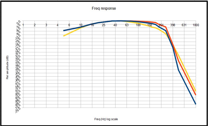
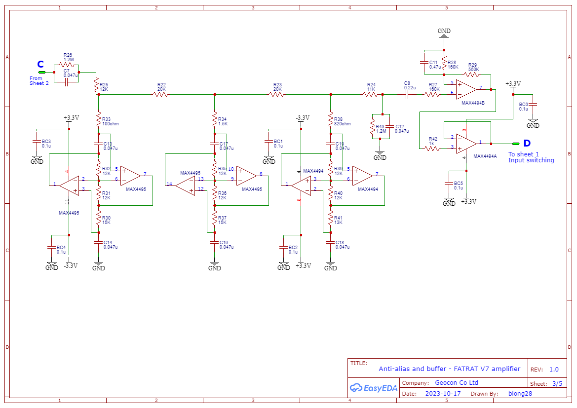
Sheet 3 : Anti-alias and final buffer
This is quite a complex part of the circuit as the anti-alias filter is a 3 stage filter using 2 amplifiers in each stage. Stages 1 and 2 use a MAX4495 and stage 3 uses a MAX4494. Both of these IC's are the same in design just the packaging provides 4 amplifiers for the MAX4495 whilst only 2 amplifiers for the MAX4494.
The output of this last part of the amplifier is routed back to the input switching circuit to be directed to the ADC.
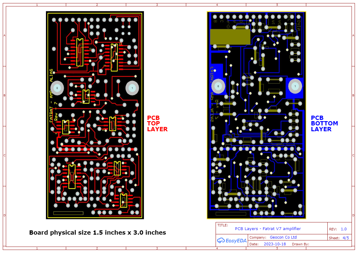
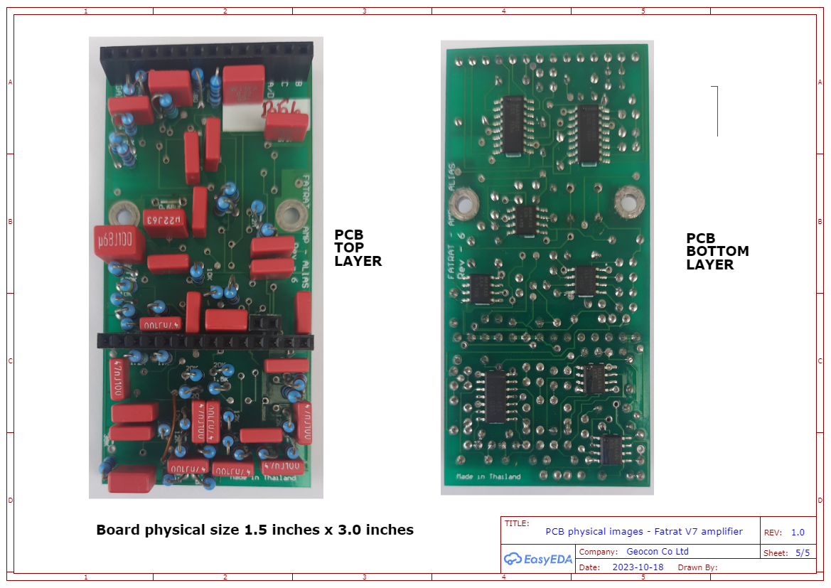
Sheets 4 & 5 : PCB images
These images are of the actual PCB layers for the board design and a physical image of the amplifier itself.
It is designed to be a daughter type card of some 3 x 1.5 inches to be mounted on a carrier baord via 2 rows of 0.1 inch spaced pins. The design has the IC's mounted on one side and the other side supports the placement of capacitors and resistors. This design makes for easy removal of IC's if necessary. Also resistors are mounted in a vertical manner to allow for better component packing density.
The amplifier is designed for an ADC system sampling at 1 millisecond. Theoretical anti-alias should be at 250Hz however design allows for frequencies up to around 320Hz with very steep roll off.